Power Electronics Simulations
1)
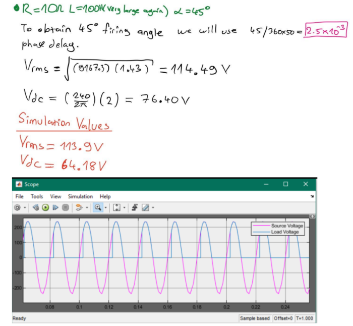
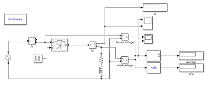
In the given single-phase half wave rectifier circuit, the load current i0=Ia is assumed to be constant, with a very large load inductance (L) chosen by your selection, operating at a frequency of 50 Hz.
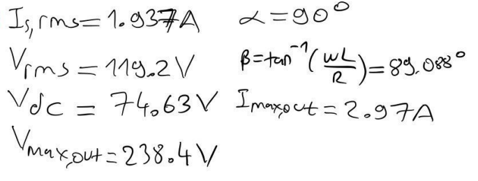
(a) Simulation for α = 90°:
For α = 90°, the load voltage waveform v0 can be simulated. Considering R = 10 Ω, the average value Vdc of the load voltage waveform can be calculated based on the obtained graphs. This simulation allows us to observe the output voltage under these specific conditions. Theoretical calculations can also be performed to verify the results obtained from the simulation.
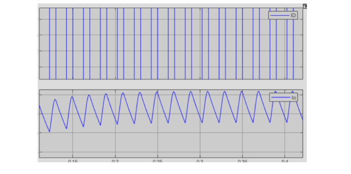
(b) Simulation for R = 10 Ω and α = 45°:
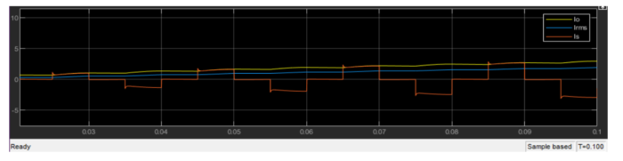
In this scenario, with R = 10 Ω and α = 45°, the average output current can be simulated. By adjusting the firing angle, the output current waveform can be observed and analyzed to understand the impact of the change in α on the output current.
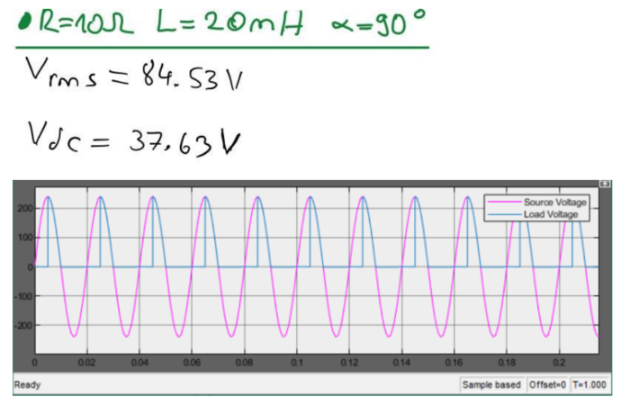
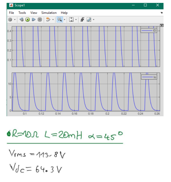
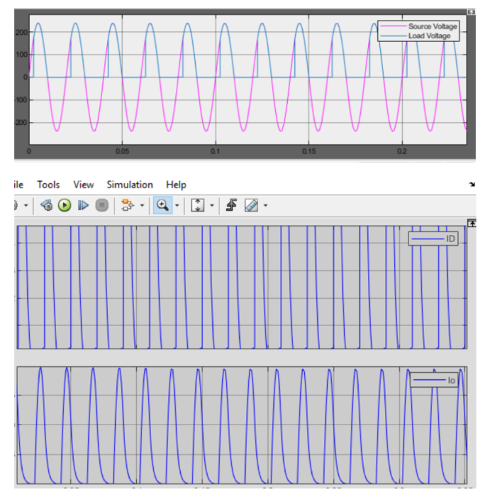
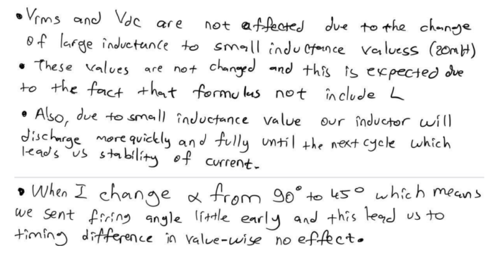
(c) Simulation with Load Inductance of 20 mH:
When the load inductance is reduced to 20 mH, the voltage and current waveforms at the output, input, and semiconductor devices can be simulated. By comparing these waveforms with the ones obtained in the case of large inductance, the differences can be noted and analyzed. Changes in waveforms could be due to the altered inductance, allowing us to comprehend the effects on the rectifier operation and efficiency.
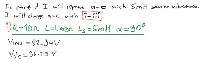
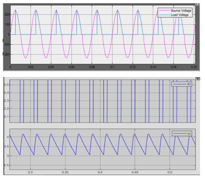
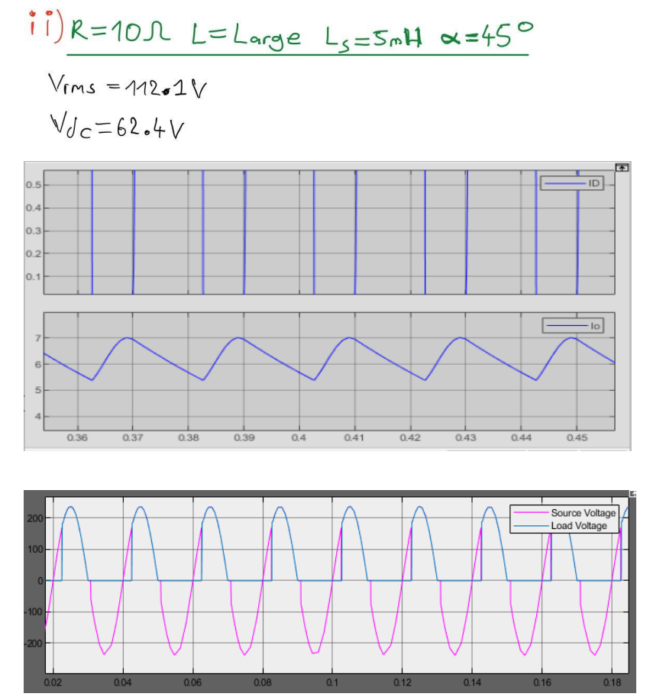
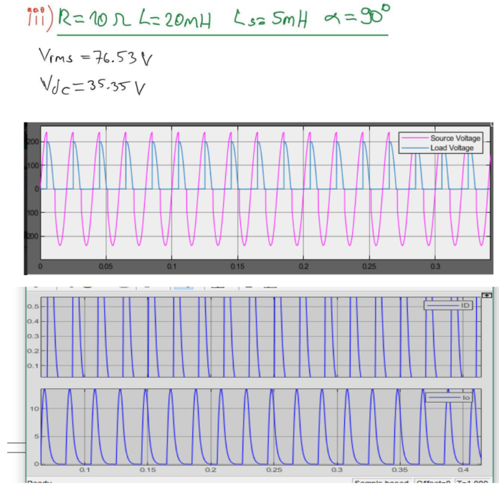
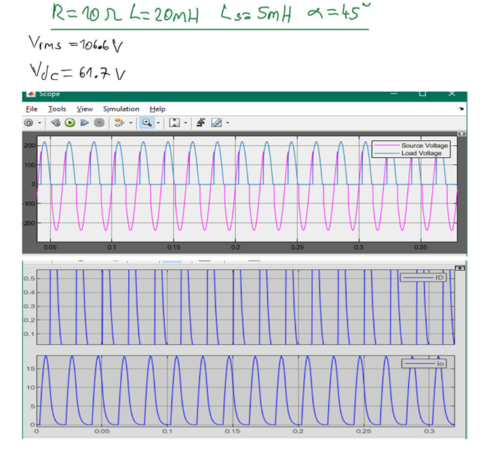
(d) Simulation with 5 mH Source Inductance:
Introducing a source inductance of 5 mH into the rectifier circuit requires a repetition of the simulations conducted in parts (a) to (c). The voltage and current waveforms at the output, input, and semiconductor devices need to be simulated and analyzed. The presence of source inductance can significantly affect the performance of the rectifier, and observing these changes is crucial for understanding the real-world implications. Through these simulations and analyses, a comprehensive understanding of the rectifier’s behavior under different conditions can be gained. This knowledge is essential for designing efficient rectifier circuits.
Design
(a)
(b)
(c)
(d)

2)
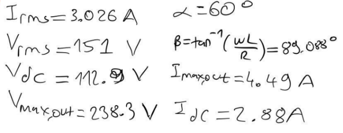
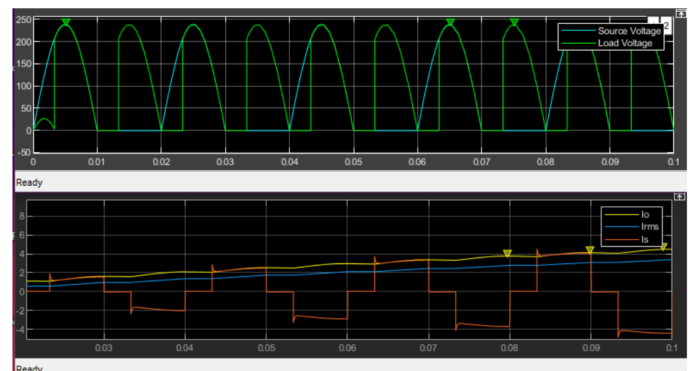
In the given half-wave controlled rectifier circuit with an R-L load supplied from a 312 V source at 50 Hz and a delay angle of α = 45°, we will simulate the load voltage and current characteristics for different cases to understand the variations in the system behavior.
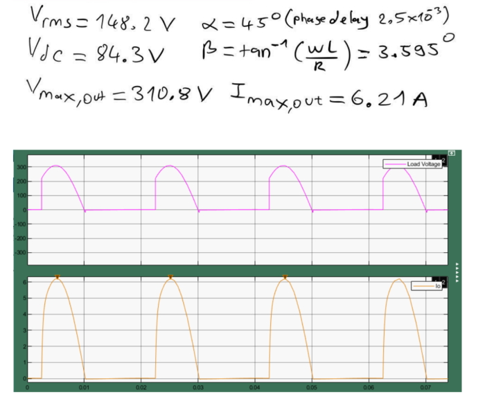
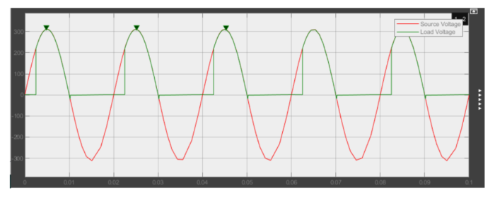
(a) R = 50 Ω, L = 10 mH:
In this scenario, with a moderate resistance of 50 Ω and relatively low inductance of 10 mH, the load voltage and current waveforms will be simulated. By observing these waveforms, we can analyze how the system responds to these parameters. The higher resistance and lower inductance will influence the current and voltage dynamics differently than in other cases.
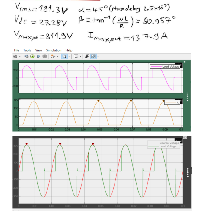
(b) R = 0.5 Ω, L = 10 mH:
Here, the resistance is significantly reduced to 0.5 Ω while maintaining the same inductance as in the previous case. The low resistance implies a more conductive path for the current, potentially leading to higher current values. Simulating the load voltage and current in this scenario will allow us to observe the impact of extremely low resistance on the system behavior.
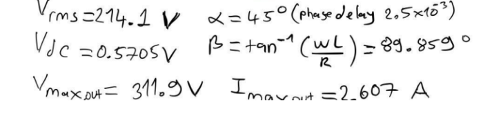
(c) R = 0.5 Ω, L = 650 mH:
In this case, the inductance is significantly increased to 650 mH while maintaining the low resistance of 0.5 Ω. The high inductance implies a strong opposition to the change in current, which can significantly affect the current and voltage waveforms. Simulating the load voltage and current for these parameters will help us understand the impact of high inductance on the rectifier’s behavior, especially in combination with low resistance.
By comparing and contrasting the voltage and current waveforms for these different cases, we can gain insights into how resistance and inductance values influence the performance of the rectifier. Analyzing the differences among these cases will provide valuable information for optimizing the design of rectifier circuits based on specific load requirements and system constraints.
Design
(a)
(b)
(c)
Comment:
From the values I obtained, our phase delay is 2.5×10^-3. Current increase from part a to b since our Z decreased maximum current increased dramatically, also Vrms is increased. In part c Vrms also increased but this time current decreased dramatically since our Z is increased. Also when I increased inductance we can see that graphs become more unstable.
3)
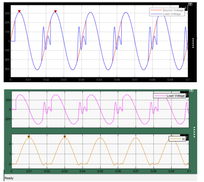
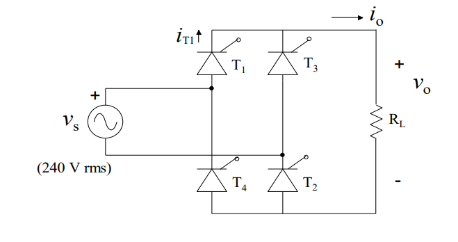
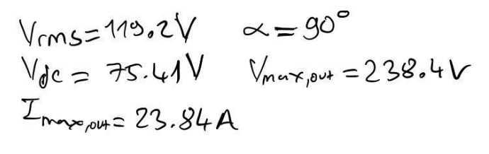
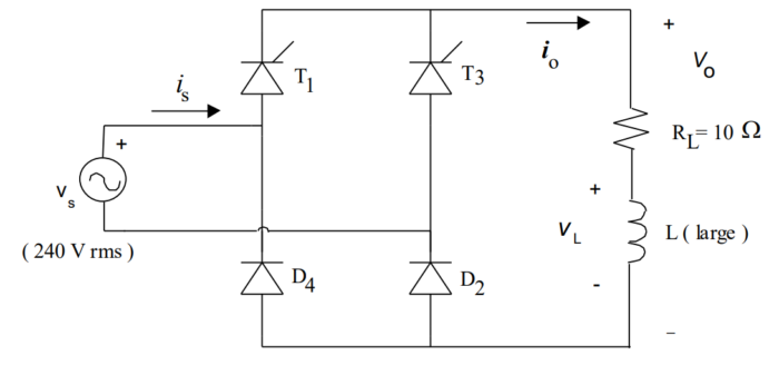
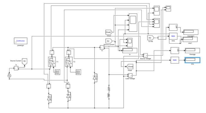
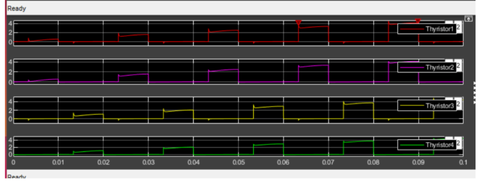
In the given single-phase fully-controlled bridge converter scenario, the system consists of a resistive load (RL=10Ω) powered by a 240 V rms 50 Hz AC source. The converter operates with a firing angle α=90°. The objective is to simulate the output voltage (v0) and the current through each thyristor, and then verify the relationship between the input current graphically.
Design

Comment:
This circuit has only Resistor with Thyristors. From graphs we can see that all of them started at the same time due to no charging, discharging case (No L component). Also I can see that there is no negative part in the graphs. We have four thyristors in our design and T1, T2 thyristors fired together and T3, T4 fired together. Voltage can be controlled by controlling firing angle of Thyristors.
4)
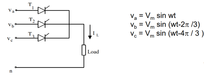
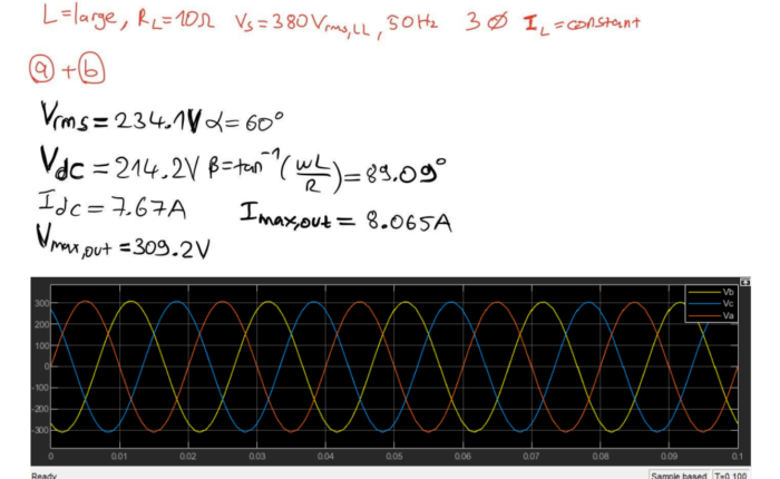
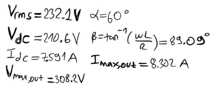
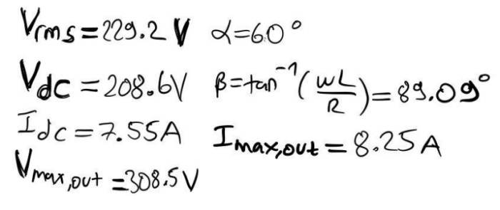
In the given scenario of a three-phase controlled midpoint converter supplying power to a highly inductive load (RL=10Ω) from a 380 V rms (line-to-line), 50 Hz, three-phase source, where the load current (IL) is constant, let’s perform the following simulations and analyses. Simulation and Analysis:
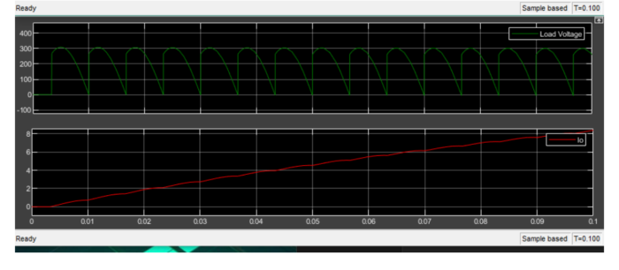
(a) Simulate Load Voltage Waveform for α=π/3:
In this scenario, the load voltage waveform will be simulated for a firing angle α=π/3. The load voltage waveform will be affected by the controlled switching of the converter, and observing this waveform will provide insights into the output characteristics.
(b) Simulate Average Load Current for α=π/3:
With α=π/3, the average load current will be simulated. This involves calculating the average value of the load current waveform under these specific conditions. Understanding the average load current is crucial for assessing the power delivery to the load.
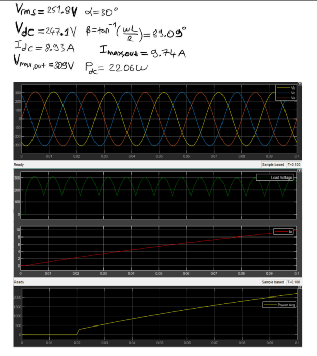
(c) Simulate Average Power Supplied to the Load for α=π/6:
For α=π/6, the average power supplied to the load will be simulated. By determining the average power, we can comprehend the efficiency of power transfer and the converter’s performance in delivering power to the load.
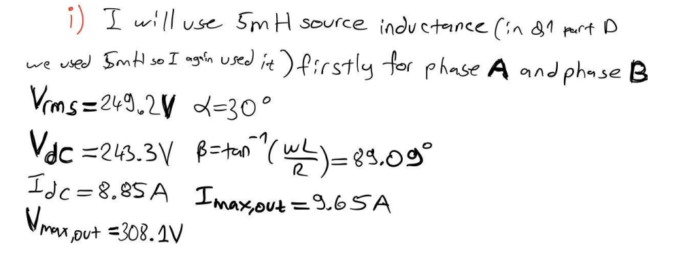
(d) Generate Source Inductances:
For Only A and B Phases: Introducing source inductances for only A and B phases will change the characteristics of the input power supply. Simulating the output voltage and current under these conditions will allow us to observe how the absence of inductance in one phase affects the system behavior.
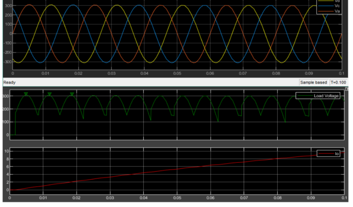
For All Phases: Comparing this scenario with the previous one (only A and B phases having inductance) will provide a comprehensive understanding of how the presence of inductance in all phases influences the output voltage and current characteristics. Analyzing these differences will help in assessing the impact of inductance on the overall system performance.
Design
(a) & (b)
(c)
(d)
Comment:
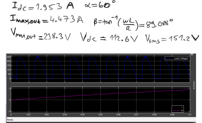
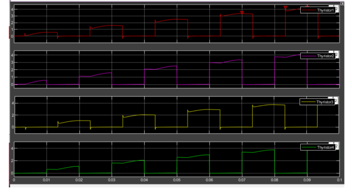
We have three phase midpoint converter, we have large inductance at load in part a and b I simulated circuit with α=60 and in part c I simulated the circuit with α=30 and if I compare both of them I can see that load voltage and current increased in graph-wise not much changed. In part d first I added source inductance of 5mH to phase A and B then all phases. In case all phases has source inductance, has lower output voltage and current than 2 phases case, and we can see commutation happens between phase changes.
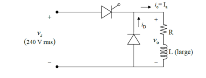
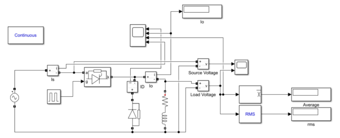
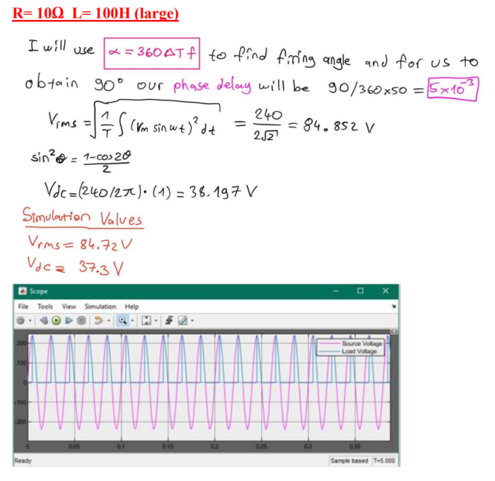
5)
Single-phase half-controlled bridge converter supplying power to a highly inductive load (RL=10Ω) from a 240 V rms 50 Hz AC source, considering a firing angle α=60°.
Initial Simulation for α=60°:
In this scenario, the output voltage and current waveforms will be simulated for a firing angle α=60°. The large inductance (L is chosen to be significant) and the specified resistance (RL=10Ω) will influence the waveforms significantly. By controlling the firing angle, the behavior of the converter can be observed under these specific conditions. The output voltage and current waveforms will reveal the effect of the inductive load on the system dynamics.
Simulation of Source Current for α=90° and RMS Value Calculation:
For α=90°, the source current waveform will be simulated. The RMS value of the source current can be calculated graphically by squaring the waveform values, averaging them, and then taking the square root of the result. This RMS value represents the effective current flowing from the source when the firing angle is set at α=90°. Analyzing this value provides insights into the average power drawn from the source.
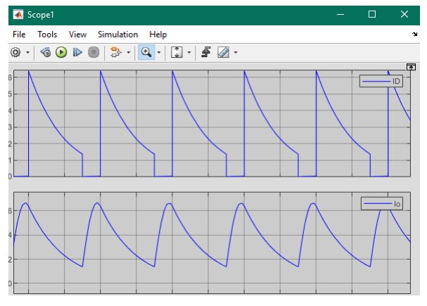
Simulation with Freewheeling Diode:
Upon adding a freewheeling diode parallel to the load, the load and current characteristics will be simulated again. The freewheeling diode provides a path for the inductive current to circulate when the main thyristors are off, reducing voltage spikes and ensuring a smoother current flow. Comparing these characteristics with the initial simulation (without the diode) will highlight the differences in terms of voltage spikes, current fluctuations, and overall stability of the system.
Design
(a)
(b)
(c)
Comment:
In part a the load voltage get below zero but rest it stayed positive in Part c when I added free wheeling diode due to its negative part killing feature the voltage didn’t get below zero. Moreover, due to free-wheeling diode load current become more stable comparing with part a, and the maximum output current increased, also Vdc increased.